DIY Electronics
Simple electronics as a hobby
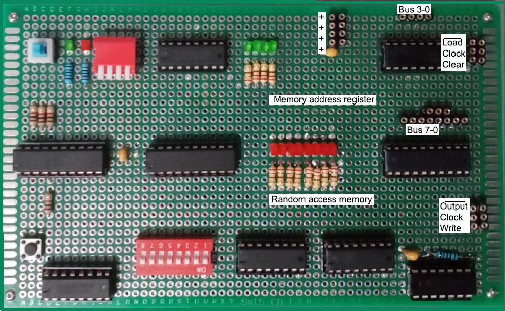
Building an 8-bit pcb computer
This project is largely based on the project with the name "Building an 8-bit breadboard computer" from Ben Eater ( website ). His videos explaining the build in detail are available on YouTube.Video shows multiplication 12 x 12 with intermediate results at a speed of 11 Hz. Explanation of code is right here.
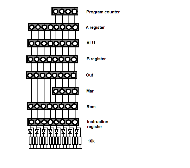
A general discription
A clock is needed to synchronize all operations, especially the communication between different units inside the CPU and with memory. It works like a metronome, every 'tick' or clock cycle the CPU performs a specific set of predetermined operations.The program counter PC keeps track of the next step in a program to be executed. A (conditional) jump in a program changes the PC to another step, like a goto statement.
The memory address register stores the address from which data will be fetched or data will be stored in RAM.
Random access memory (RAM) stores the instructions and values necessary to run a program. A 4 bit memory address means you can define max. 16 instructions (op-codes) including operands. When output is enabled RAM puts the data pointed to by the address in the memory address register on the bus or when write is enabled it reads the data from the bus and stores it at that address.
The instruction register reads the instructions data from the bus. The 8 bits in this register are divided into 4 upper bits holding the op-code and 4 lower bits holding the operand (either a memory address or a value). The 4 upper bits are connected to the control unit, ready to be executed at the next clock pulse. The 4 lower bits are put back on the bus when output is enabled by the control unit.
The A and B registers are just two storage places in the CPU of which each can hold 8 bits of data temporarily, like operands in an arithmetic operation.
The arithmetic and logic unit or ALU performs simple arithmetic and logic operations. In our case it can only add and subtract 8 bit values of the A and B register. If the result is greater than 255 (decimal) or less than zero it wraps around.
The output unit reads data from the bus and displays the number value on three 7-segments displays. The forth 7-segments display shows the minus sign if two's complement is desired and the value is negative. A timer and EEprom are used to decode and multiplex the binary data input to 4 displays of the decimal value.
Finally the control unit takes the instruction data of 4 bits from the instruction register combined with a counter that counts from 0 to 4 as input and outputs 16 bites of data to enable certain features of other units. It has its own clock to activate control lines to other units before they get triggered by the general clock.
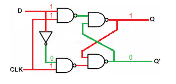 This image shows how a D-Type flipflop remembers 1 bit of data. With each clock pulse the status of D (1 or 0) will be propagated to output Q. Without clock pulse no change.
A register, capable of storing 8 bits of data, is based on 2 4-Bit D-Type flipflops.
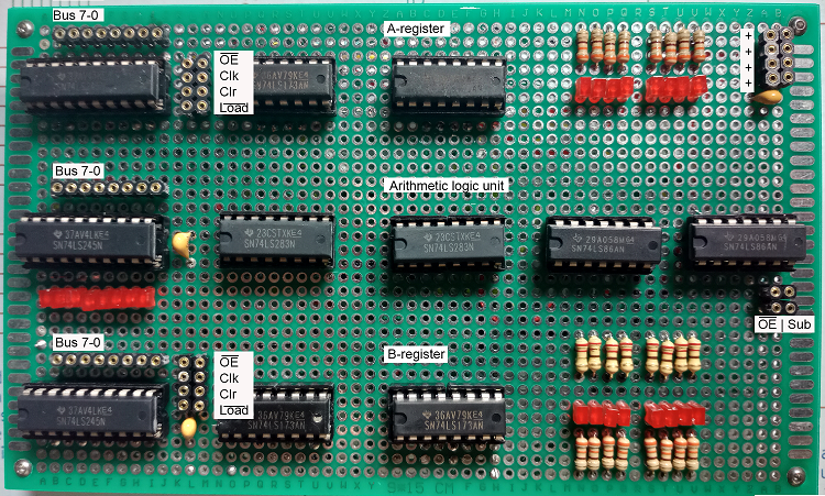 A-register, ALU and B-register.
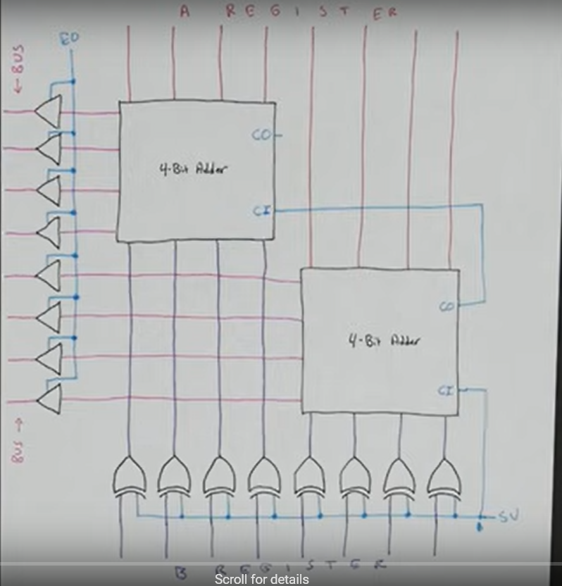 Schematic shows how the ALU works together with A and B register including subtraction by two's complement using XOR gates and carry bit.
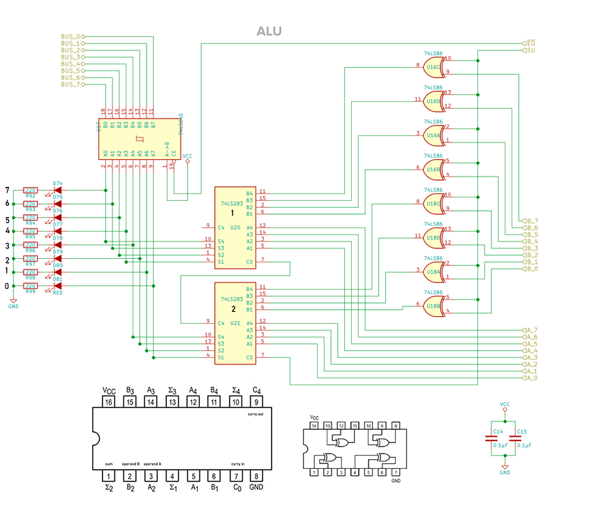 ALU module with pinouts and removed flags register.
 MAR and RAM modules combined.
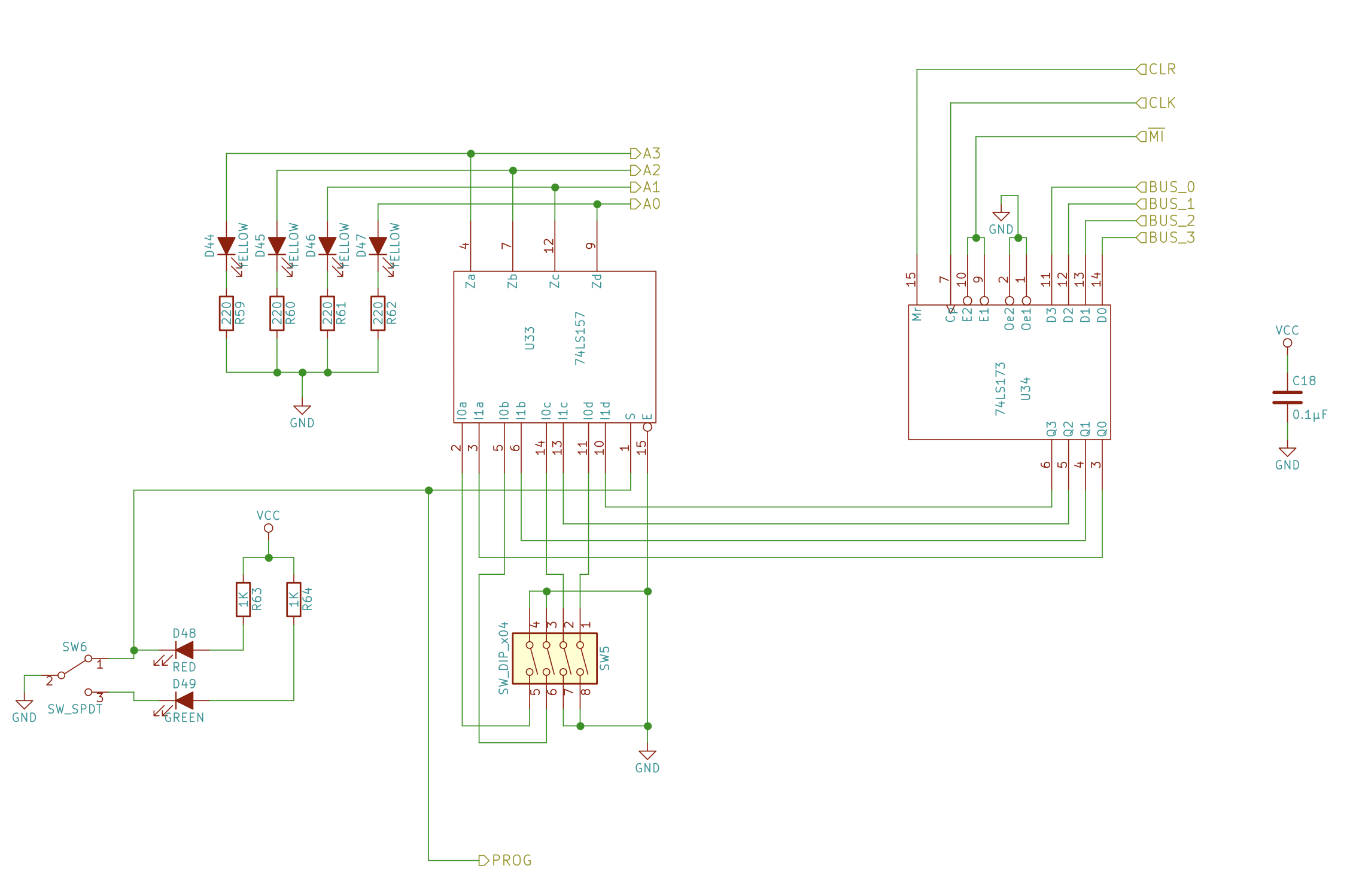 Memory address register.
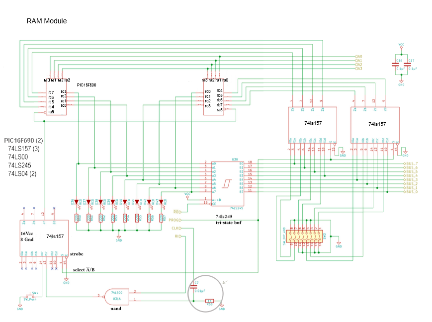 Ram module using mcu PIC16f690 (2x) instead of the hard to obtain 74LS189 (2x)
The capacitor/resistor combination to shorten the clock pulse when writing data from the bus to RAM distorts the clock signal with a negative effect on the ALU, so I bypassed the capacitor/resistor (see gray circle). >>> Code for PIC16f690 <<<
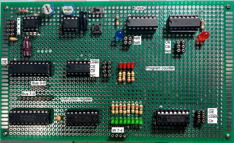 Clock, Program counter and Instruction register. The clock is wired to PC and IR and not an input.
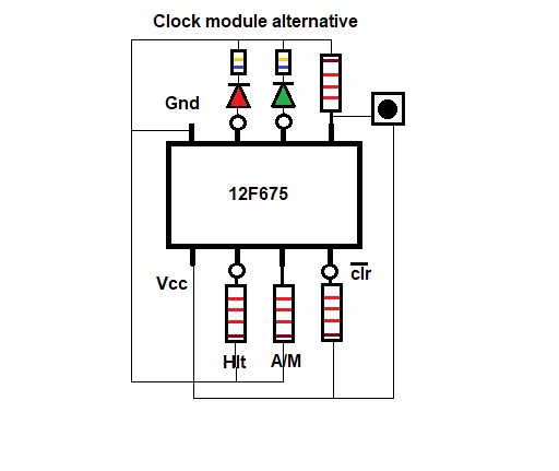 This PIC12F675 generates a clock signal. GP2 was defined as external interrupt, but turned out to be too sensitive and is now just a regular input. It will stop the clock immediately. To restart the clock press the button to MCLR (GP3). A switch determines manual or automatic running of the clock at 11 hertz. The limit switch is to advance the clock manually.
>>> Code for the clock <<<
This PIC12F675 generates a clock signal. GP2 was defined as external interrupt, but turned out to be too sensitive and is now just a regular input. It will stop the clock immediately. To restart the clock press the button to MCLR (GP3). A switch determines manual or automatic running of the clock at 11 hertz. The limit switch is to advance the clock manually.
>>> Code for the clock <<<
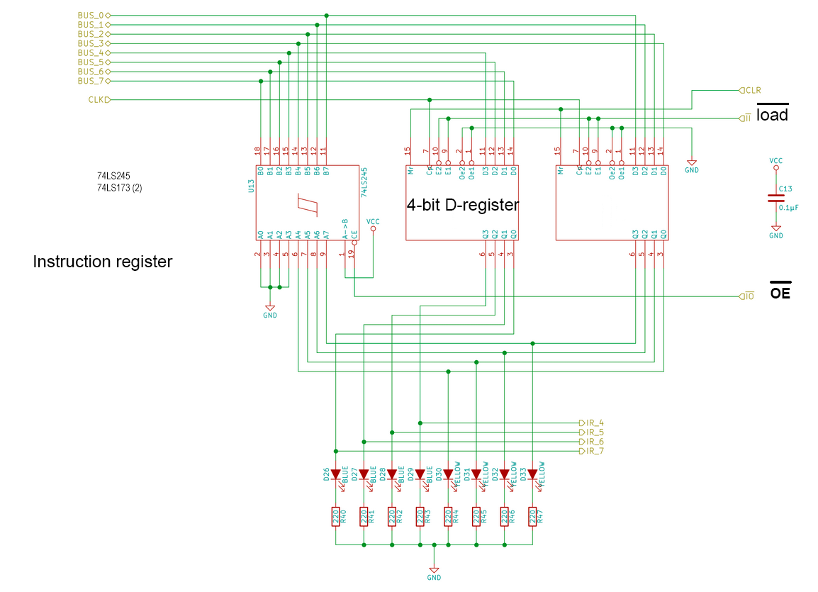 Instruction register.
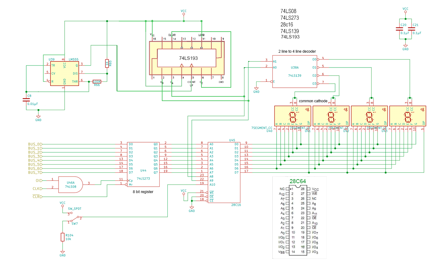
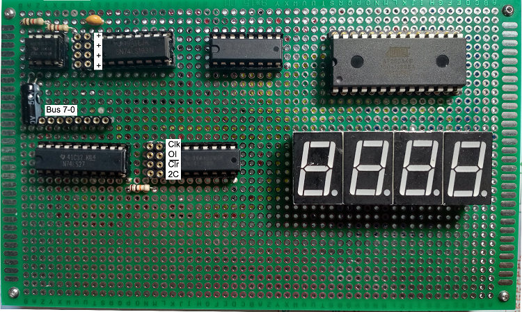 Output module
 Output module using a 74LS193 instead of a 74ls76
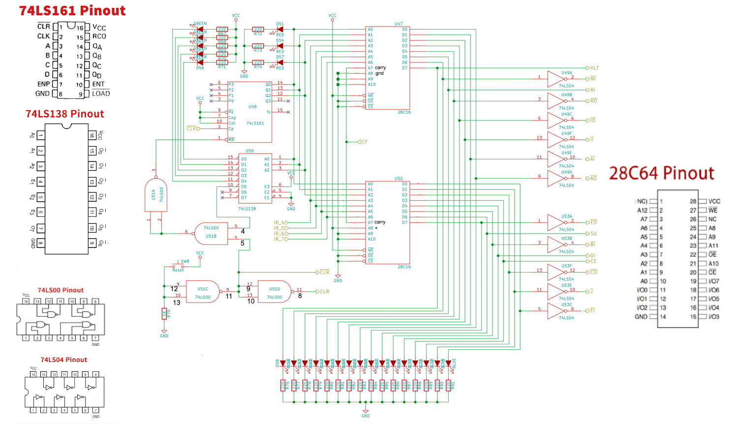
 Modified control module pinout.
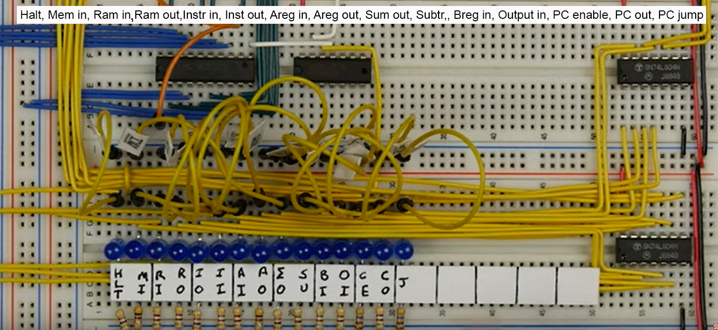 Which control output goes where. Ram in (RI) is called write. What is missing is the pin 16 going to flag register in (FI).
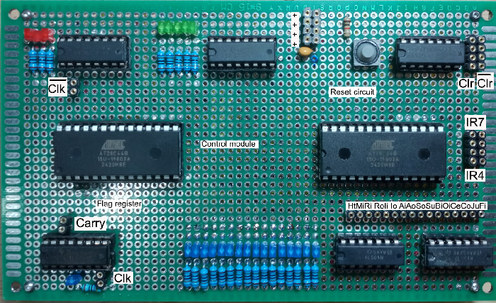
 Modified control unit, including carry flag register and reset circuit
 Bus connections. The 10K pull-down resistors should be 2.2K. Higher values interfere with the working of the RAM module with the 2 pics.
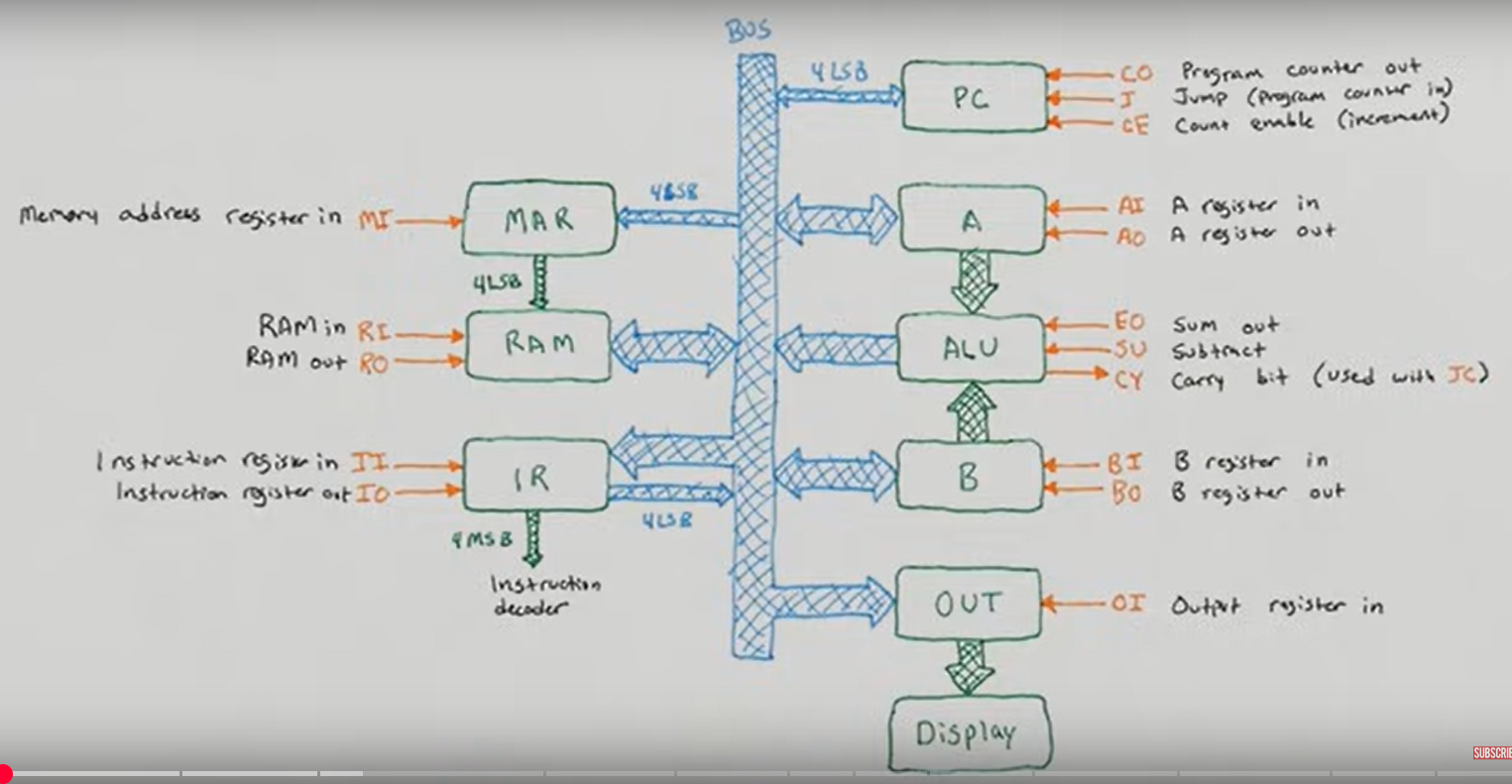 Bus architecture
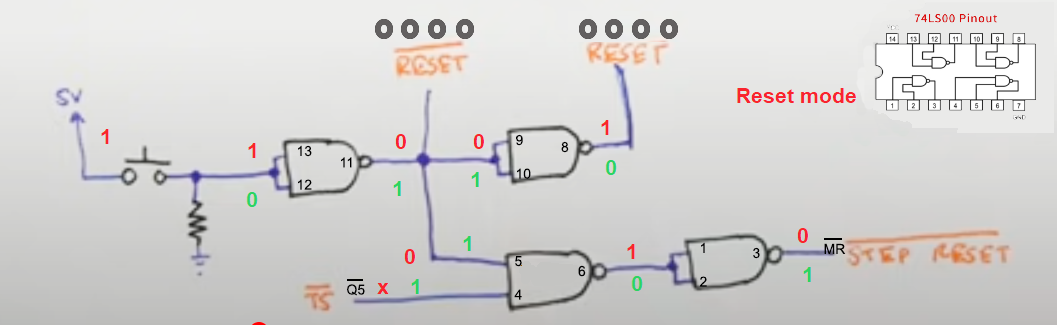 Reset circuit
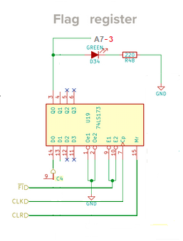 Carry flag register.
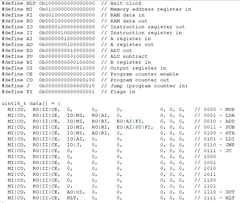 Micro and operational codes defined.
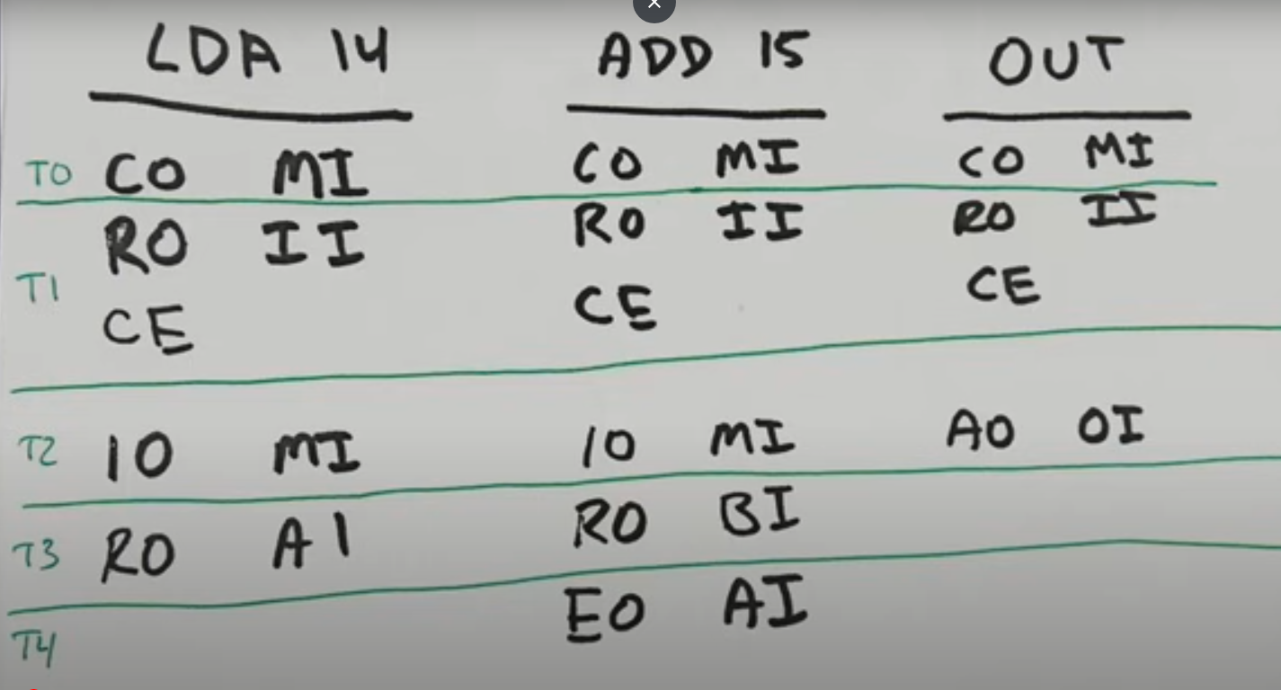 Microcode to load, add and display 2 numbers at memory addresses 14 and 15.
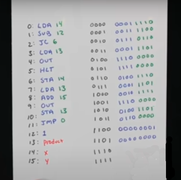 Op-codes for multiplication.
The multiplication of 2 numbers uses all available address space
and all but one opcodes.
Op-codes for multiplication.
The multiplication of 2 numbers uses all available address space
and all but one opcodes.At memory address 14 and 15 are the two values stored (Multiplicand × Multiplier) for multiplication.
| Addr 0: LDA 14 | copy value at address 14 from RAM into A-register |
| Addr 1: SUB 12 | copy value at address 12 (one) into B-register and subtract this leads to a carry output captured in the carry flag register, unless the A-register has a value of zero then there will be no carry out. |
| Addr 2: JC 6 | if carry flag register has a value of one (carry set) the op-code leads to a PC jump to step 6. |
| Addr 3: LDA 13 | copy value at address 13 from RAM into A-register (starts with zero). |
| Addr 4: OUT | show value in LDA on 7-segment displays. |
| Addr 5: HLT | stop the clock and therefore the program. |
| Addr 6: STA 14 | store the value of A-register into RAM address 14 (X - 1). |
| Addr 7: LDA 13 | copy value at address 13 from RAM into A-register |
| Addr 8: ADD 15 | copy value at address 15 (Y) into B-register and add |
| Addr 9: OUT | show value in LDA on 7-segment displays (Y; 2Y; 3Y .. XY) |
| Addr 10: STA 13 | store the value of A-register into RAM address 13. |
| Addr 11: JMP 0 | PC is set to zero. |
| Addr 12: | has a value of 1 |
| Addr 13: | the result of each addition. |
| Addr 14: | Multiplier X |
| Addr 15: | Multiplicand Y |
I used the following table to trace every step of a multiplication going wrong.
| ADDR | OC | OP | INST | OPER | Control lines |
| 0000 | LDA | 14 | 0001 | 1110 | MI|CO, RO|II|CE, IO|MI, RO|AI |
| 0001 | SUB | 12 | 0011 | 1100 | MI|CO, RO|II|CE, IO|MI, RO|BI, EO|AI|SU|FI |
| 0010 | JC* | 6 | 0111 | 0110 | MI|CO, RO|II|CE, IO|J |
| 0011 | LDA | 13 | 0001 | 1101 | MI|CO, RO|II|CE, IO|MI, RO|AI |
| 0100 | OUT | 1110 | 0000 | MI|CO, RO|II|CE, AI|OI | |
| 0101 | HLT | 1111 | 0000 | MI|CO, RO|II|CE, HLT | |
| 0110 | STA | 14 | 0100 | 1110 | MI|CO, RO|II|CE, IO|MI, AO|RI |
| 0111 | LDA | 13 | 0001 | 1101 | MI|CO, RO|II|CE, IO|MI, RO|AI |
| 1000 | ADD | 15 | 0010 | 1111 | MI|CO, RO|II|CE, IO|MI, RO|BI, EO|AI|FI |
| 1001 | OUT | 1110 | 0000 | MI|CO, RO|II|CE, AI|OI | |
| 1010 | STA | 13 | 0100 | 1101 | MI|CO, RO|II|CE, IO|MI, AO|RI |
| 1011 | JMP | 0 | 0110 | 0000 | MI|CO, RO|II|CE, IO|J |
| 1100 | 1 | ||||
| 1101 | product | ||||
| 1110 | multiplier | ||||
| 1111 | multiplicant | ||||
| * if carry set |
Simulate control unit
 Instead of the EEPROM based control unit a PIC16F887 runs the control lines and clock as a way to test the other modules. This test showed problems with the IR register (solder joint failure) and catching the carry bit at the right time.
>>> the control unit simulated by pic16f887 <<<
Instead of the EEPROM based control unit a PIC16F887 runs the control lines and clock as a way to test the other modules. This test showed problems with the IR register (solder joint failure) and catching the carry bit at the right time.
>>> the control unit simulated by pic16f887 <<<
4-bit multiplier
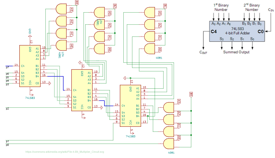 This 4-Bit mutiplier uses three Full-Adders and 16 AND-Gates.
The diagram was copied from commons.wikimedia.org, and corrected!
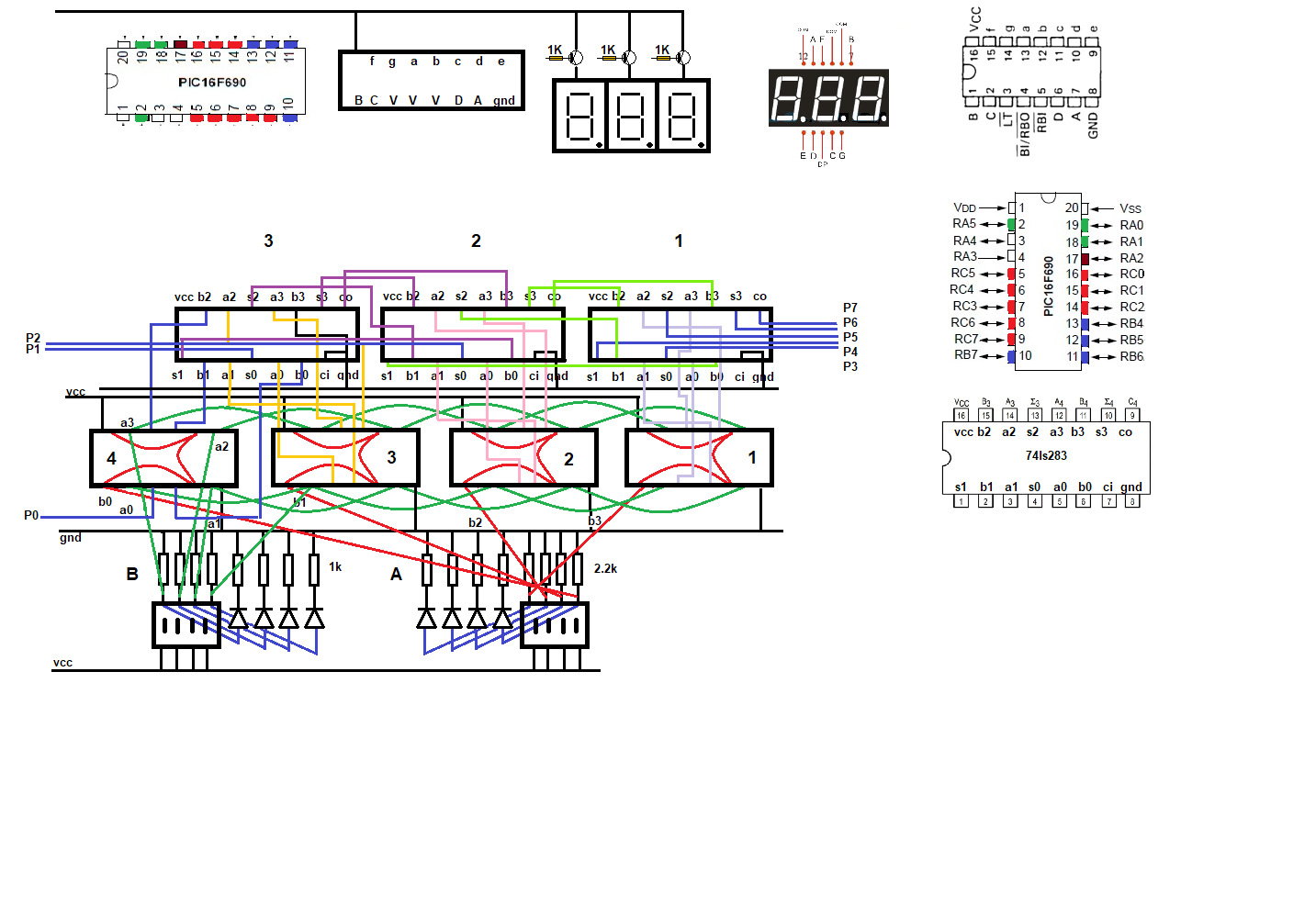
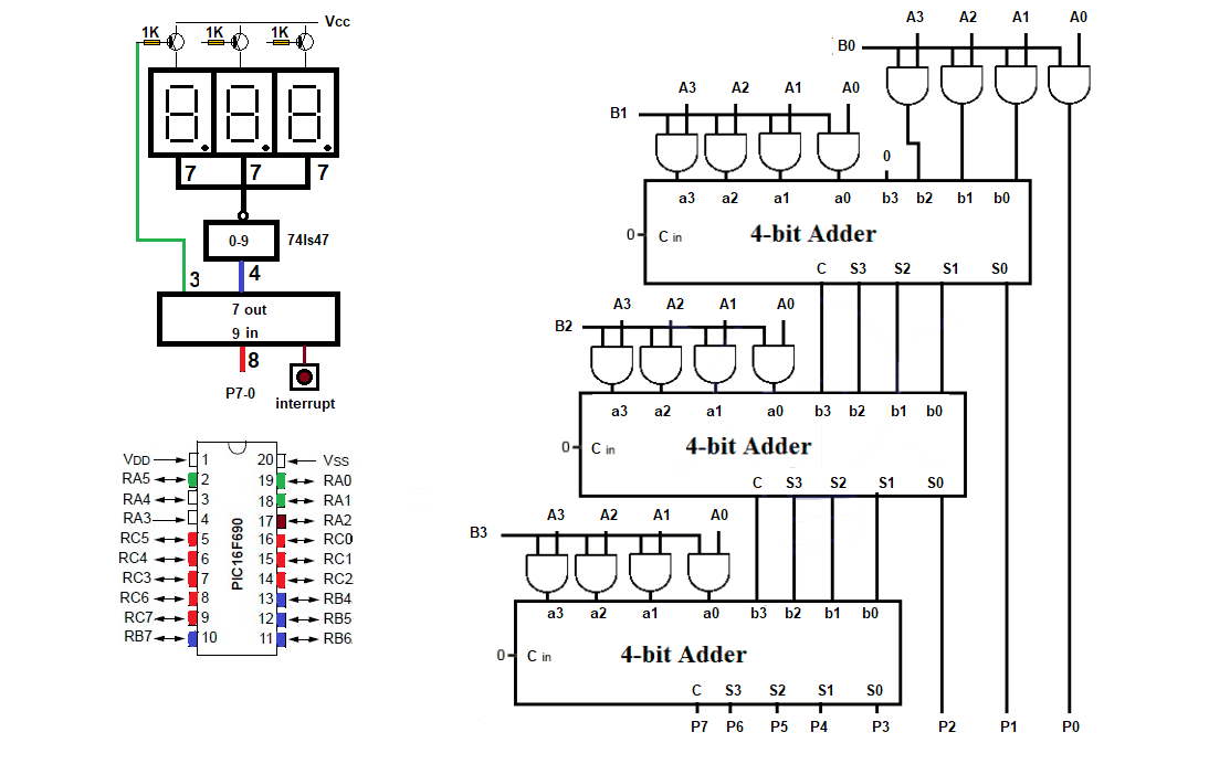 Schematic of a 4-bit multiplier with pic16f690 controlled output.
>>> Code for PIC16f690 <<<
Schematic of a 4-bit multiplier with pic16f690 controlled output.
>>> Code for PIC16f690 <<<
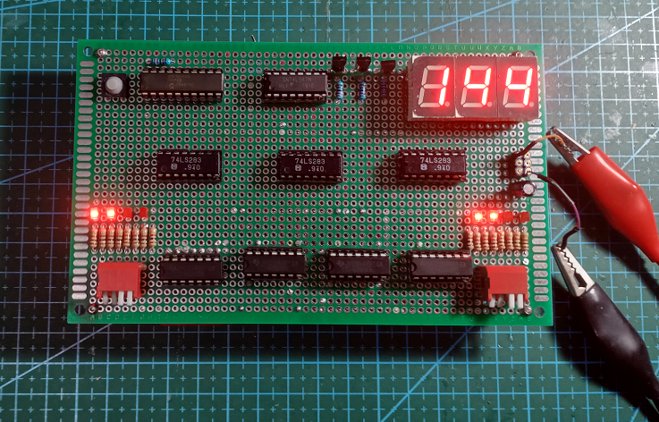 12x12=144